Learn C with me - week 5 - memory pt. 1
table of contents
Memory is often overlooked aspect of the computer. It’s the crucial part of this device and without it we wouldn’t even be able to call the computer well, a computer. Machine to be turing complete requires some sort of memory either in form of long tape as in original idea of turning machine or silly little logic gates made out of few nanometer transistors to store processed data.
from transistor to data
If you don’t care about low-level details of computer memory feel free to skip ahead to the next post covering memory management in C, however if you ever wondered how data is really stored on the hardware then you found a good place! So let’s begin.
1. transistors

This 4 inch in diameter silicone wafer contains probably billions or even trillions of single transistors in form of chips. In case of computer parts, transistors are very small (usually in range 128nm to even 3nm in newer chips like apple’s M3) switches which can be either turned on or off. They have usually 3 wires, 2 for the input and 1 for the output and are triggered by amount of power which varies along with size of the transistor itself. The smaller transistor is the less power it usually requires to trigger, so naturally all tech industry is aiming to build as small transistors as possible to make devices even more power efficient and even faster. However transistors are pretty useless standalone and this is the moment where logic gates come in.
2. logic gates
Few transistors can be connected together in particular order to create logic gates. Logic gate is piece of hardware being able to perform certain task if condition is met which in case of logic gates can be roughly translated to example “if power in wire A and B is on then return 1” as in AND gate. We can distinguish few basic logic gates such as NOT, AND, OR, XOR, NAND and NOR. Each of this comes with own truth table which is table where all input possibilities are displayed along with expected output. Here are truth tables for previously mentioned logic gates: 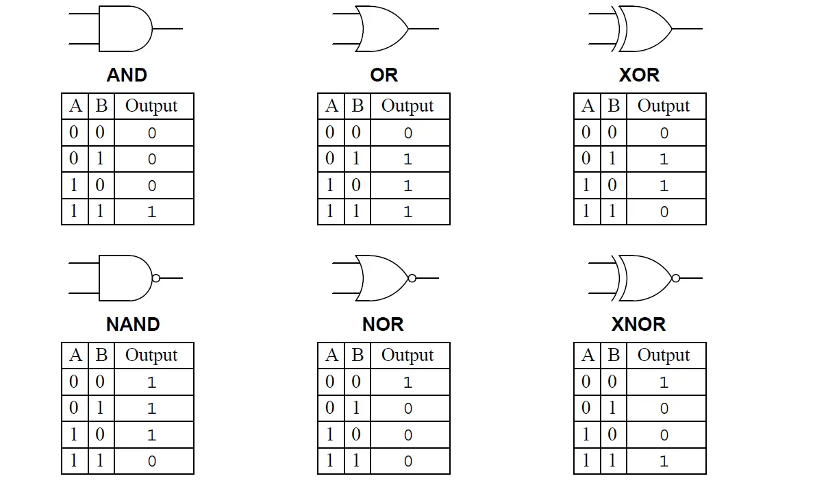 Truth table for 6 types of logic gates
3. latch memory
Once we have all required logic gates, then we can connect them to create latch memory circuit, which is able to store single bit value (either 0 or 1) as long as power is being supplied to hold it. Latch memory has not 1 or 2, but actually 3 input wires, where first is the power supply, second is the state flag for switching memory from read to write mode and the third one is for supplying value we want to store. Below is simple chart presenting this circuit made out of logic gates:
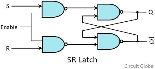
Diagram showing structure of memory latch from logic gates
4. memory cells
We already achieved something, but storing single bit is not really useful, at least for us. To expand storage capabilities of our memory, we have to connect 8 single bit latch memory circuits into one single-byte memory cell like in the diagram below: 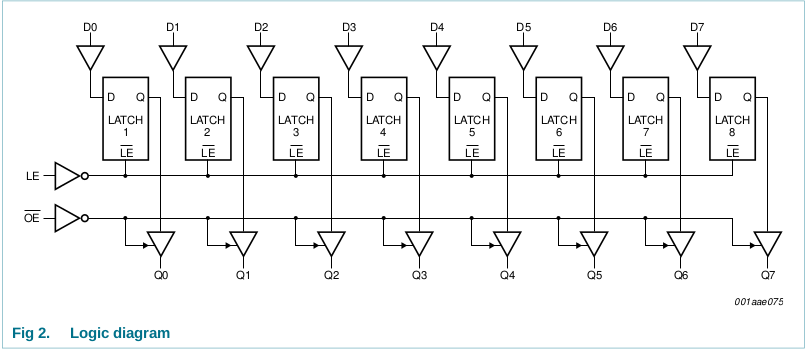
Now, instead of 3 inputs and 1 output we have 10 inputs and 8 outputs, for each bit of data.
5. byte matrix
As you can see, the amount of wires grows in fast pace and if we wanted to have just 4 bytes of memory to store integer number, we would need 40 wires for input and 32 wires for output! It’s quite insane, isn’t it? Think how many wires we would need to build just 2gb ram chip or as in most powerful machines out there - whopping 128gb ram unit - i guess that amount of wires would run in millions if not in billions. Fortunately, clever people invented memory matrix to access one cell at the time, but with far lower amount of wires. So how it works? Usually memory cells are placed in 2 dimensional grid (however, with today’s technology we can already create even 3 dimensional matrixes), with fixed amount of rows and columns. Each row and column requires 1 wire to connect to memory cell and these wires are counted in some order, so we introduced memory addressing because to access memory cell, we have to know its exact position on the matrix. In our simplified example memory matrix holds 64 memory cells, with 8 rows and 8 columns, so the address for example will look like this: 0d17 which doesn’t mean “access 17th memory cell” but rather “access memory cell at row 1 and column 7” which in our case would give us path to the 16th memory cell in the array. Okay, but what about wires? Now we are doing far better! Instead of 10 input and 8 output wires for each memory cell, which would give us 640 inputs and 512 outputs for 64 memory cells, we just have as usually wire for power, for flag and 8 wires for value, but also additional 16 for wiring rows and columns. Thanks to this trick we went from 640 inputs to just 26 inputs and from 512 outputs to just 24 outputs. Such a cost savings! Whats’s more - ram matrix is managed by unit called multiplexer or mux for short which is so far the coolest sounding component. Isn’t it?
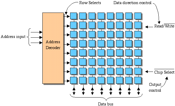
Diagram of ram memory matrix created from address decoder (multiplexer) and single byte memory cells
6. memory banks
Have you ever seen physical RAM from the computer?
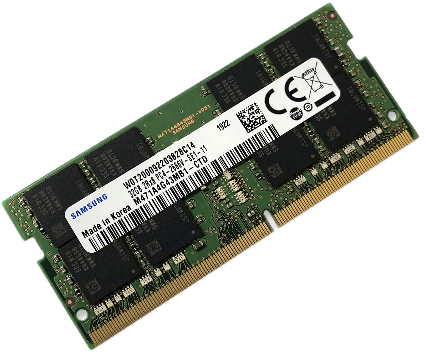 As you can see, there is many of this weird black rectangles. They are nothing more than memory arrays we just covered but on far larger scale. Often containing tens of thousands or even hundreds of thousands of memory cells. But how they are connected? Each of this memory banks is connected to the physical memory management chip which works like traffic lights, constantly orchestrating data flow between these banks and not without a reason! After zooming out a bit, we will see another piece required to connect memory even further to the cpu and also again, save some wires along the way.
7. memory bus
Many memory banks are connected to the same path called bus. Thanks to this trick, we can significantly reduce usage of wires, since all memory banks share same output and input wires, which are managed by the memory controller to avoid collisions and in worst case data loss, which is inacceptable in such mission critical device as personal computer. Just imagine being operated for brain cancer and doctor just sits and says “sorry, I can’t access data about which region of your brain we need to extract, I will just put back your skull and next week we will see you on the appointment to examine your brain once again”. While this is an extreme example, it’s very likely to happen as our world including healthcare goes every day closer to the full digitalisation of data. Similarly to ram matrix the memory bus is also managed by the multiplexer.
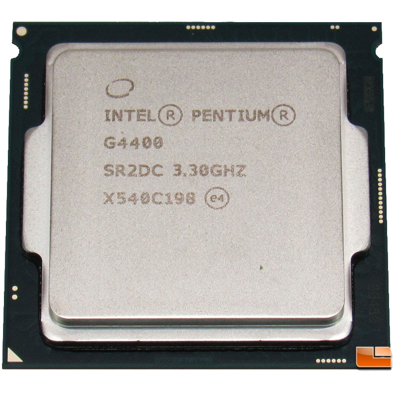
8. cpu
Below photo of CPU with IHS on it for better heat disposal.
Before data is being processed by the cpu itself, first it has to be loaded to cpu’s memory which is way faster than RAM. Inside CPU there are two types of memory; the first one are registers - small data boxes with size depending on the cpu architecture, measured in bits. For example the 32 bit cpu has 32 bit registers (4 byte each) while 64 bit cpu has 64 bit registers (8 bytes each). What’s more - many modern processors have even registers specialised in storing floating point numbers. Hint: it’s related to maximum variable size and size of memory pointers in C. The second type of CPU built-in memory is cache, often with many levels labeled L1, L2 and L3. Cache is meant to store often accessed data to save time and keep it ready to use without the need for additional jump to much slower RAM. The number of cache means its speed and often the size. While L1 cache is usually the fastest one, the L3 cache will most likely have the most space for storing data. I would love to explain how caching works, unfortunately I have to admit that it’s the one of the few architecture elements beyond my understanding and for now algorithms and technology behind caching remains magic to me.
9. operating system
Unless you are developing embedded code or the operating system itself from scratch, then probably your code will rely on the virtual memory provided by gnu/linux, windows or any other unix-like system. Working principle of the virtual memory is quite simple. It acts as a bridge between program’s code and physical memory somewhere inside computer. When you launch program through an operating system, then operating system looks for unused space inside memory, often fragmented and in many pieces, then maps addresses to these free spaces and tricks a program into thinking it got pretty decent chunk of continuous and homogeneous memory.
You can see simple visualisation of it on the table below:
| what program sees | real memory address |
|---|---|
| … | … |
| 0x100000100000 | 0x7ffdeebc9430 |
| 0x100000100001 | 0x7ffdeebc9431 |
| 0x100000100002 | 0x7ffdeebc9432 |
| 0x100000100003 | 0x8ffdefbc1501 |
| 0x100000100004 | 0x8ffdefbc1503 |
| … | … |
| 0x400000100000 | 0x2a9bc18e5f8 |
| 0x400000100001 | 0x2a9bc18e5f9 |
| 0x400000100002 | 0x2a9bc18e5fa |
| 0x400000100003 | 0x2a9bc18e5fb |
| 0x400000100004 | 0x2a9bc18e5fc |
| … | … |
Virtual memory also serves as protection mechanism against any attempt to access memory which doesn’t belongs to the program which wants to see or modify it. Thanks to this every time some poorly designed program crashes it doesn’t corrupt other program’s memory or while malicious program tries to access our encryption keys it gets prevented from obtaining secret information (at least until it obtains root privileges) however it’s worth keeping in mind that this attribute of virtual memory also can be double edged sword. If by some reason you will try to get outside memory allocated to you by operating system or you go too far with memory pointer, then execution of the code will be interrupted by the segmentation fault.
summary
Hopefully after reading this post you know more about computer memory than initially.
I’m glad if you went through this whole post and I want to thank to every person who read all of this with excitment before finishing final draft.
Keep coding, keep learning and have a nice day… if you can find one.
Laura
Further reading
- how transistors work - https://www.explainthatstuff.com/howtransistorswork.html
- how logic gates work - https://www.explainthatstuff.com/logicgates.html
- logic gates wikipedia article - https://en.wikipedia.org/wiki/Logic_gate
- latch memory wikipedia article - https://en.wikipedia.org/wiki/Flip-flop_(electronics)
- virtual memory wikipedia article - https://en.wikipedia.org/wiki/Virtual_memory